mirror of
https://github.com/peter-tanner/microwave-crossover-ansys-hfss.git
synced 2024-11-30 14:20:19 +08:00
28 lines
1.4 KiB
Plaintext
28 lines
1.4 KiB
Plaintext
|
|
# Simulation of RF crossover
|
||
|
|
|
||
|
|
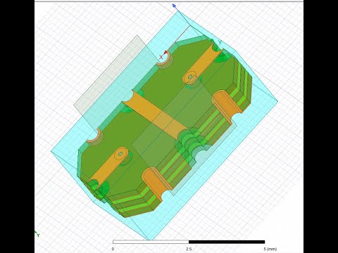
This is my first simulation in Ansys HFSS and there are some flaws I haven't fixed such as stub pads missing from the internal ground vias on the power plane.
|
||
|
|
|
||
|
|
<center><img src="assets/2023-07-13-22-24-58.png" width=400px></center>
|
||
|
|
|
||
|
|
A signal allows microwave traces to cross over each other by going through a via.
|
||
|
|
|
||
|
|
The properties of a good crossover are:
|
||
|
|
|
||
|
|
1. Good isolation between the traces crossing over
|
||
|
|
2. Low insertion loss for each of the traces
|
||
|
|
|
||
|
|
Vias are an issue as they present a discontinuity for the signal, and may result in an impedance mismatch resulting in increase in insertion loss and reflected power.
|
||
|
|
|
||
|
|
There is some amount of coupling between the two traces, which result in crosstalk.
|
||
|
|
|
||
|
|
I've made the following design considerations for manufacturing:
|
||
|
|
|
||
|
|
1. No blind vias or back-drilled vias. This is to reduce manufacturing cost and allow the device to be manufactured by JLCPCB.
|
||
|
|
2. JLCPCB 4 layer 7628 impedance controlled stackup
|
||
|
|
3. 1 - Ground/Signal plane, 2 - Ground plane, 3 - Power plane, 4 - Ground/Signal plane
|
||
|
|
4. 50 ohm impedance
|
||
|
|
|
||
|
|
I recommend you watch the following video series for an example of how to design a microwave crossover device in ansys. I used the series as a reference for my own design.
|
||
|
|
|
||
|
|
[](https://www.youtube.com/watch?v=foii4ioCV48)
|